


All STD 12 - Semicondutor electronics questions
Newest firstShowing 101–150 of 181 questions
- 101. For extrinsic semiconductors; when doping level is increased; 2021 Medium
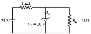
- 102. For the circuit shown below, calculate the value of \({I}_{{z}}\) : (In \({mA}\))
 2021 Medium
- 103. For the forward biased diode characteristics shown in the figure, the dynamic resistance at \({I}_{{D}}=3 \,{mA}\) will be \(.....\,\Omega\)
 2021 Medium
- 104. For the given circuit, the power across zener diode is ..... \({mW}.\)
 2021 Hard
- 105. Four \(NOR\) gates are connected as shown in figure. The truth table for the given figure is :
 2021 Hard
- 106. Given below are two statements: Statement \(I :\) \(PN\) junction diodes can be used to function as transistor, simply by connecting two diodes, back to back, which acts as the base terminal. Statement \(II :\) In the study of transistor, the amplification factor \(\beta\) indicates ratio of the collector current to the base current. In the light of the above statements, choose the correct answer from the options given below : 2021 Medium
- 107. Identify the logic operation carried out by the given circuit :-
 2021 Medium
- 108. If an emitter current is changed by \(4\, mA ,\) the collector current changes by \(3.5\, mA\). The value of \(\beta\) will be 2021 Medium
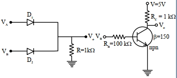
- 109. If \({V}_{{A}}\) and \({V}_{{B}}\) are the input voltages (either \(5\, {V}\) or \(0\, {V}\) ) and \({V}_{0}\) is the output voltage then the two gates represented in the following circuit \((A)\) and \((B)\) are:- \((A)\quad\quad\quad\quad(B)\)
 2021 Hard
- 110. In a given circuit diagram, a \(5 \,{V}\) zener diode along with a series resistance is connected across a \(50 \,V\) power supply. The minimum value of the resistance required, if the maximum zener current is \(90\, {mA}\) will be \(.....\,\Omega .\)
 2021 Hard
- 111. In a semiconductor, the number density of intrinsic charge carriers at \(27^{\circ} {C}\) is \(1.5 \times 10^{16} \,/ {m}^{3}\). If the semiconductor is doped with impurity atom, the hole density increase to \(4.5 \times 10^{22}\, / {m}^{3}\). The electron density in the doped semiconductor is \(.....\,\times 10^{9} / {m}^{3}\) 2021 Easy
- 112. In connection with the circuit drawn below, the value of current flowing through \(2\, k \Omega\) resistor is ............. \(\times 10^{-4} A\)
 2021 Medium
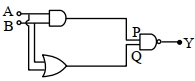
- 113. In the following logic circuit the sequence of the inputs \({A}, {B}\) are \((0,0),(0,1),(1,0)\) and \((1,1)\). The output \(Y\) for this sequence will be :
 2021 Medium
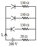
- 114. In the given figure, each diode has a forward bias resistance of \(30\, \Omega\) and infinite resistance in reverse bias. The current \({I}_{1}\) will be \(....\,A\)
 2021 Hard
- 115. \(LED\) is constructed from \(Ga-As-P\) semiconducting material. The energy gap of this \(LED\) is \(1.9\, eV\). Calculate the wavelength of light emitted and its colour. \(\left[ h =6.63 \times 10^{-34} \;Js \right.\) and \(\left. c =3 \times 10^{8}\; ms ^{-1}\right]\) 2021 Medium
- 116. Match List \(I\) with List \(II.\)
Choose the correct answer from the options given below: 2021 MediumList \(I\) List \(II\) \((a)\) Rectifier \((i)\) Used either for stepping up or stepping down the \(a.c.\) voltage \((b)\) Stabilizer \((ii)\) Used to convert \(a.c.\) voltage into \(d.c.\) voltage \((c)\) Transformer \((iii)\) Used to remove any ripple in the rectified output voltage \((d)\) Filter \((iv)\) Used for constant output voltage even when the input voltage or load current change - 117. Statement\(-I :\) By doping silicon semiconductor with pentavalent material, the electrons density increases. Statement\(-II :\) The \(n-\)type semiconductor has net negative charge. In the light of the above statements, choose the most appropriate answer from the options given below: 2021 Medium
- 118. Statement\(-I :\) To get a steady de output from the pulsating voltage received from a full wave rectifier we can connect a capacitor across the output parallel to the load \({R}_{{L}}\) Statement\(-II :\) To get a steady de output from the pulsating voltage received from a full wave rectifier we can connect an inductor in series with \({R}_{{L}}\). In the light of the above statements, choose the most appropriate answer from the options given below: 2021 Medium
- 119. The circuit contains two diodes each with a forward resistance of \(50\, \Omega\) and with infinite reverse resistance. If the battery voltage is \(6\, V\), the current through the \(120\, \Omega\) resistance is \(mA\)
 2021 Hard
- 120. The following logic gate is equivalent to
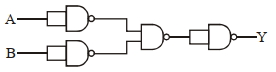 2021 Medium
- 121. The output of the given combination gates represents
 2021 Medium
- 122. The truth table for the followng logic circuit is ...... .
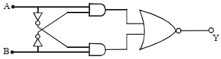 2021 Hard
- 123. The typical output characteristics curve for a transistor working in the common-emitter configuration is shown in the figure. The estimated current gain from the figure is
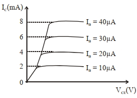 2021 Medium
- 124. The value of power dissipated across the zener diode \(\left( V _{ z }=15 V \right)\) connected in the circuit as shown in the figure is \(x \times 10^{-1}\) watt. The value of \(x ,\) to the nearest integer, is ..............
 2021 Medium
- 125. The zener diode has a \(V _{ z }=30\, V\). The current passing through the diode for the following circuit is \(\ldots \ldots \ldots \,mA.\)
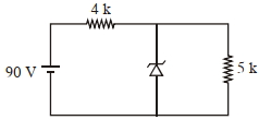 2021 Hard
- 126. Which one of the following will be the output of the given circuit?
 2021 Hard
- 127. Zener breakdown occurs in a \(p-n\) junction having \(p\) and \(n\) both : 2021 Medium
- 128. Boolean relation at the output stage\(-Y\) for the following circuit is
 2020 Medium
- 129. Both the diodes used in the circuit shown are assumed to be ideal and have negligible resistance when these are forward biased. Built in potential in each diode is \(0.7\; \mathrm{V} .\) For the input voltages shown in the figure, the voltage (in \(Volts\)) at point \(A\) is
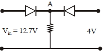 2020 Medium
- 130. Identify the operation performed by the circuit given below
 2020 Medium
- 131. If a semiconductor photodiode can detect a photon with a maximum wavelength of \(400\, nm ,\) then its band gap energy is Planck's constant \(h=6.63 \times 10^{-34}\, J . s\) Speed of ligh \(c =3 \times 10^{8}\, m / s\) 2020 Easy
- 132. In the figure, potential difference between \(A\) and \(B\) is......\(V\)
 2020 Medium
- 133. In the following digital circuit, what will be the output at \('Z',\) when the input \((A, B)\) are \((1,0), (0,0),(1,1),(0,1)\)
 2020 Hard
- 134. In the given circuit, value of \(Y\) is
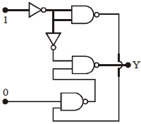 2020 Medium
- 135. The circuit shown below is working as a \(8\; \mathrm{V}\;dc\) regulated voltage source. When \(12 \;\mathrm{V}\) is used as input, the power dissipated (in \(\mathrm{mW}\) ) in each diode is (considering both zener diodes are identical)
 2020 Medium
- 136. The current \(i\) in the network is.....\(A\)
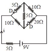 2020 Medium
- 137. The output characteristics of a transistor is shown in the figure. When \(V_{C E}\) is \(10\, V\) and \(I_{ C }=4.0\, mA ,\) then value of \(\beta_{ ac }\) is
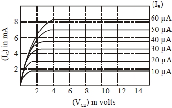 2020 Medium
- 138. Two identical capacitors \(\mathrm{A}\) and \(\mathrm{B}\), charged to the same potential \(5\; \mathrm{V}\) are connected in two different circuits as shown below at time \(\mathrm{t}=0\) If the charge on capacitors \(A\) and \(B\) at time \(\mathrm{t}=\mathrm{CR}\) is \(\mathrm{Q}_{\mathrm{A}}\) and \(\mathrm{Q}_{\mathrm{B}}\) respectively, then (Here \(e\) is the base of natural logarithm)
 2020 Medium
- 139. When a diode is forward biased, it has a voltage drop of \(0.5\, V.\) The safe limit of current through the diode is \(10\, mA\). If a battery of emf \(1.5\, V\) is used in the circuit, the value of minimum resistance to be connected in series with the diode so that the current does not exceed the safe limit is\(.....\Omega\) 2020 Medium
- 140. With increasing biasing voltage of a photodiode, the photocurrent magnitude 2020 Medium
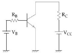
- 141. A common emitter amplifier circuit, built using an \(npn\) transistor, is shown in the figure. Its \(dc\) current gain is \(250\), \(R_C = 1\,k\, \Omega \) and \(V_{CC} = 10\,V\). What is the minimum base current for \(V_{CE}\) to reach saturation?.........\(\mu A\)
 2019 Medium
- 142. An \(NPN\) transistor is used in common emitter configuration as an amplifier with \(1\,k\Omega \) load resistance. Signal voltage of \(10\,mV\) is applied across the base emitter. This produces a \(3\,mA\) change in the collector current and \(15\,\mu A\) change in the base current of the amplifier. The input resistance and voltage gain are 2019 Hard
- 143. An \(npn\) transistor operates as a common emitter amplifier, with a power gain of \(60\, dB\). The input circuit resistance Is \(100\,\Omega \) and the output load resistance is \(10 \,k\,\Omega \). the common emitter current gain \(\beta \) is 2019 Hard
- 144. Figure shown a \(DC\) voltage regulator circuit, with a Zener diode of breakdown voltage \(= 6\,V\). If the unregulated input voltage varies between \(10\, V\) to \(16\, V\), then what is the maximum Zener current ?.......\(mA\)
 2019 Medium
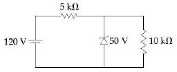
- 145. For the circuit shown below, the current through the Zener diode is......\(mA\)
 2019 Medium
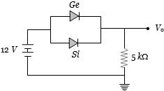
- 146. Ge and Si diodes conduct at \(0.3 \,V\) and \(0.7\, V\) respectively. In the following figure if Ge diode connection are reversed, the valve of \(V0\) changes by.....\(V\)
 2019 Hard
- 147. In the figure, given that \(V_{BB}\) supply can vary from \(0\) to \(5.0 \,V,\,\,V_{CC} = 5\,V,\) \(\beta _{dc} = 200,\,\,R_B = 100,\,k\Omega ,\) \(R_C = 1\,k\Omega \) an \(V_{BE} = 1.0\,V,\) The minimum base current and the input voltage at which the transistor will go to saturation, will be respectively
 2019 Hard
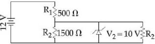
- 148. In the given circuit the current through Zener Diode is close to.......\(mA\)
 2019 Medium
- 149. Mobility of electron in a semiconductor is defined as the ratio of their drift velocity to the applied electric field. If, for an \(n-\) type semiconductor, the density of electrons is \(10^{19}\, m^{-3}\) and their mobility is \(1.6\, m^2\,/(V.s)\) then the resistivity of the semiconductor(since it is an \(n-\) type semiconductor contribution of holes is ignored) is close to ................ \(\Omega m\) 2019 Medium
- 150. The circuit shown below contains two ideal diodes, each with a forward resistance of \(50\,\Omega \). If the battery voltage is \(6\,V\), the current through the \(100\,\Omega \) resistance (in Amperes) is
 2019 Medium
No questions on this page match these filters.