


Topics
7 topics- 50Qs Boolean Algebra and Logic Gates Most asked
- 42Qs PN Junction and Diode
- 34Qs Zener Diode
- 10Qs Light Emitting Diode (L.E.D), Photodiode, Solar Cell
- 11Qs Types Semiconductors
- 2Qs Application of junction diode (Rectifier)
- 32Qs Junction Transistor
All STD 12 - Semicondutor electronics questions
Newest firstShowing 1–50 of 181 questions
- 1. A diode has Zener voltage of \(10\) V and maximum power dissipation of \(0.5\) W, then the minimum resistance to be used in series with this diode for safety when it is connected to a \(25\) V power supply is ______ \(\Omega\). 2026 Easy
- 2. A voltage regulating circuit consisting of Zener diode, having break-down voltage of 10 V and maximum power dissipation of 0.4 W , is operated at 15 V . The approximate value of protective resistance in this circuit is _________ \(\Omega\). 2026 Easy
- 3. Assuming in forward bias condition there is a voltage drop of 0.7 V across a silicon diode, the current through diode \(D _1\) in the circuit is ___________mA . (Assume all diodes in the given circuit are identical)
 2026 Hard
- 4. Consider a circuit consisting of a capacitor (\(20\ \mu\)F), resistor (\(100\ \Omega\)) and two identical diodes as shown in figure. The resistance of diode under forward biasing condition is \(10\ \Omega\). The time constant of the circuit is \(\alpha \times 10^{-3}\) s. The value of \(\alpha\) is _____
 2026 Medium
- 5. Find the correct combination of A, B, C and D inputs which can cause the LED to glow
 2026 Hard
- 6. For the given logic circuit, which of the following inputs combination will make both LED\(-1\) and LED\(-2\) to glow?
 2026 Medium
- 7. For the given logic gate circuit, which of the following is the correct truth table?
 2026 Medium
- 8. Given below are two statements: one is labelled as Assertion A and the other is labelled as Reason R
Assertion A: A diode under reverse-biased condition provides very small current which is nearly independent of voltage until a critical limit at which the current increases drastically.
Reason R: Below the critical voltage limit, only majority charge carriers flow which increases drastically above critical voltage.
Choose the correct answer from the options given below 2026 Medium - 9. Identify the correct truth table of the given logical circuit.
 2026 Medium
- 10. If \(X\) and \(Y\) are the inputs, the given circuit works as _______.
 2026 Easy
- 11. In a semiconductor p-n diode, the doping concentrations on p-side and n-side are \(10^{15}\text{ atoms/cm}^3\) and \(10^{18}\text{ atoms/cm}^3\), respectively. Which one of the following statements is true ? 2026 Medium
- 12. Refer to the logic circuit given below. For two inputs \((A=1, B=1)\) and \((A=0, B=1)\), output \((Y)\) will be __________.
 2026 Medium
- 13. The charge stored by the capacitor C in the given circuit in the steady state is _________ \(\mu C\).
 2026 Medium
- 14. The correct truth table for the given input data of the following logic gate is:
 2026 Medium
- 15. The following diagram shows a Zener diode as a voltage regulator. The Zener diode is rated at \(V _{ Z }=5 V\) and the desired current in load is 5 mA . The unregulated voltage source can supply upto 25 V . Considering the Zener diode can withstand four times of the load current, the value of resistor \(R _{ S }\) (shown in circuit) should be ___________ \(\Omega\).
 2026 Easy
- 16. The given circuit works as :
 2026 Easy
- 17. The maximum rated power of the LED is \(2\) mW and it is used in the circuit with input voltage of \(5\) V as shown in the figure below. The current through resistance \(R_S\) is \(0.5\) mA. The minimum value of the resistance of \(R_S\), to ensure that the LED is not damaged is _______ k\(\Omega\).
 2026 Hard
- 18. Two \(4\) bits binary numbers, \(A = 1101\) and \(B = 1010\) are given in the inputs of a logic circuit shown in figure below. The output \((Y)\) will be:
 2026 Medium
- 19. Two p-n junction diodes \(D _1\) and \(D _2\) are connected as shown in figure. A and B are input signals and C is the output. The given circuit will function as a ___________.
 2026 Hard
- 20. A zener diode with 5 V zener voltage is used to regulate an unregulated dc voltage input of 25 V. For a \(400 \Omega\) resistor connected in series, the zener current is found to be 4 times load current. The load current \(\left(I_L\right)\) and load resistance \(\left(R_{\mathrm{L}}\right)\) are : 2025 Easy
- 21.

\(\begin{array}{c|c|c} A & B & Y \\\hline 0 & 0 & 1 \\0 & 1 & 1 \\1 & 0 & 0 \\1 & 1 & 1\end{array}\)
To obtain the given truth table, following logic gate should be placed at G : 2025 Easy - 22. Consider a n-type semiconductor in which \(\mathrm{n}_{\mathrm{e}}\) and \(\mathrm{n}_{\mathrm{h}}\) are number of electrons and holes, respectively.
(A) Holes are minority carriers
(B) The dopant is a pentavalent atom
(C) \(\mathrm{n}_{\mathrm{e}} \mathrm{n}_{\mathrm{h}} \neq \mathrm{n}_{\mathrm{i}}^2\)
(where \(n_i\) is number of electrons or holes in semiconductor when it is intrinsic form)
(D) \(\mathrm{n}_{\mathrm{e}} \mathrm{n}_{\mathrm{h}} \geq \mathrm{n}_{\mathrm{i}}^2\)
(E) The holes are not generated due to the donors Choose the correct answer from the options given below : 2025 Easy - 23. Consider the following logic circuit.

The output is \(\mathrm{Y}=0\) when : 2025 Medium - 24. Consider the following statements:
A. The junction area of solar cell is made very narrow compared to a photo diode.
B. Solar cells are not connected with any external bias.
C. LED is made of lightly doped p-n junction.
D. Increase of forward current results in continuous increase of LED light intensity.
E. LEDs have to be connected in forward bias for emission of light.
Choose the correct answer from the options given below: 2025 Easy - 25.
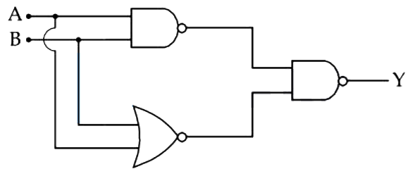
For the circuit shown above, equivalent GATE is : 2025 Easy - 26. In the following circuit, the reading of the ammeter will be : (Take Zener breakdown voltage \(=4 \mathrm{~V})\)
 2025 Medium
- 27. Refer to the circuit diagram given in the figure. which of the following observations are correct?
A. Total resistance of circuit is \(6 \Omega\)
B. Current in Ammeter is 1 A
C. Potential across \(A B\) is 4 Volts.
D. Potential across CD is 4 Volts
E. Total resistance of the circuit is \(8 \Omega\).
Choose the correct answer from the options given below: 2025 Medium
- 28. The Boolean expression \(\mathrm{Y}=\mathrm{A} \overline{\mathrm{B}} \mathrm{C}+\overline{\mathrm{A}} \overline{\mathrm{C}}\) can be realised with which of the following gate configurations.
A. One 3-input AND gate, 3 NOT gates and one 2input OR gate, One 2-input AND gate,
B. One 3-input AND gate, 1 NOT gate, One 2input NOR gate and one 2-input OR gate
C. 3-input OR gate, 3 NOT gates and one 2-input AND gate
Choose the correct answer from the options given below. 2025 Medium - 29. The output of the circuit is low (zero) for:

(A) \(\mathrm{X}=0, \mathrm{Y}=0\)
(B) \(X=0, Y=1\)
(C) \(X=1, Y=0\)
(D) \(\mathrm{X}=1, \mathrm{Y}=1\)
Choose the correct answer from the options given below : 2025 Easy - 30. The output voltage in the following circuit is : (Consider ideal diode case)
 2025 Medium
- 31. What is the current through the battery in the circuit shown below?
 2025 Easy
- 32. Which of the following circuits represents a forward biased diode?

Choose the correct answer from the options given below : 2025 Easy - 33. A light emitting diode \((LED)\) is fabricated using GaAs semiconducting material whose band gap is \(1.42 \mathrm{eV}\). The wavelength of light emitted from the \(LED\) is _______. 2024 Hard
- 34. A potential divider circuit is connected with a DC source of \(20 \mathrm{~V}\), a light emitting diode of glow in voltage \(1.8 \mathrm{~V}\) and a zener diode of breakdown voltage of \(3.2 \mathrm{~V}\). The length (PR) of the resistive wire is \(20 \mathrm{~cm}\). The minimum length of \(P Q\) to just glow the LED is _______ cm.
 2024 Hard
- 35. A Zener diode of breakdown voltage \(10 \mathrm{~V}\) is used as a voltage regulator as shown in the figure. The current through the Zener diode is _______.
 2024 Hard
- 36. Conductivity of a photodiode starts changing only if the wavelength of incident light is less than \(660 \mathrm{~nm}\). The band gap of photodiode is found to be \(\left(\frac{x}{8}\right) \mathrm{eV}\). The value of \(x\) is _______. (Given, \(\mathrm{h}=6.6 \times 10^{-34} \mathrm{Js}, \mathrm{e}=1.6 \times 10^{-19} \mathrm{C}\) ) 2024 Hard
- 37. Following gates section is connected in a complete suitable circuit. For which of the following combination, bulb will glow \((ON)\)?
 2024 Hard
- 38. Identify the logic gate given in the circuit.
 2024 Hard
- 39. Identify the logic operation performed by the given circuit.
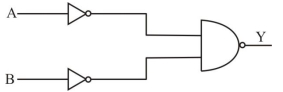 2024 Hard
- 40. In series \(LCR\) circuit, the capacitance is changed from \(\mathrm{C}\) to \(4 \mathrm{C}\). To keep the resonance frequency unchanged, the new inductance should be _______. 2024 Hard
- 41. In the given circuit if the power rating of Zener diode is \(10 \mathrm{~mW}\), the value of series resistance \(R_s\) to regulate the input unregulated supply is _______.
 2024 Hard
- 42. In the given circuit, the breakdown voltage of the Zener diode is \(3.0 \mathrm{~V}\). What is the value of \(\mathrm{I}_z\) ?
 2024 Hard
- 43. In the given circuit, the voltage across load resistance \(\left(R_L\right)\) is _______.
 2024 Hard
- 44. The acceptor level of a p-type semiconductor is \(6 \mathrm{eV}\). The maximum wavelength of light which can create a hole would be _______. (Given hc \(=1242 \mathrm{eV} \mathrm{nm}\).) 2024 Hard
- 45. The \(I-V\) characteristics of an electronic device shown in the figure. The device is _______.
 2024 Hard
- 46. The output of the given circuit diagram is _______.
 2024 Hard
- 47. The output \(\mathrm{Y}\) of following circuit for given inputs is _______.
 2024 Hard
- 48. The truth of the given circuit diagram is _______.
 2024 Hard
- 49. The truth table for this given circuit is _______.
 2024 Hard
- 50. The value of net resistance of the network as shown in the given figure is _______.
 2024 Hard
No questions on this page match these filters.
Frequently asked
How many STD 12 - Semicondutor electronics questions came in JEE Mains?
181 questions from 2013–2026, each with the correct answer and a full solution.
Which STD 12 - Semicondutor electronics topic is asked the most?
Boolean Algebra and Logic Gates, with 50 questions, followed by PN Junction and Diode with 42.
How difficult are STD 12 - Semicondutor electronics questions?
12% are easy, 56% medium and 32% hard.