MHT CET · Physics · Semiconductors
To obtain the truth-table shown, from the following logic circuit, the gate \(\mathrm{G}\) should be
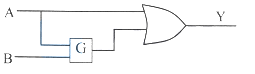
\(\begin{array}{|l|l|l|}\hline \mathrm{A} & \mathrm{B} & \mathrm{Y} 0 & 0 & 1 0 & 1 & 0 1 & 0 & 1 1 & 1 & 1 \\\hline\end{array}\)
- A AND
- B NAND
- C OR
- D NOR
Answer & Solution
Correct Answer
(D) NOR
Step-by-step Solution
Detailed explanation
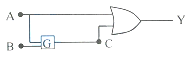
The truth table for given configuration is as shown below.
\(\begin{array}{|c|c|c|c|c|}
\hline Case & \mathbf{A} & \mathbf{B} & \mathbf{C} & \mathbf{A}+\mathbf{C}=\mathrm{Y} \\
\hline I & 0 & 0 & \mathrm{C}_1 & 0+\mathrm{C}_1=1 \\
\hline II & 0 & 1 & \mathrm{C}_2 & 0+\mathrm{C}_2=0 \\
\hline III & 1 & 0 & \mathrm{C}_3 & 1+\mathrm{C}_3=1 \\
\hline IV & 1 & 1 & \mathrm{C}_4 & 1+\mathrm{C}_4=1 \\
\hline
\end{array}\)
Considering case (I), in order to have output \(\mathrm{Y})\) as \(1, \mathrm{C}_1\) has to be 1 . For input values, \(\mathrm{A}=0\) and \(\mathrm{B}=0\), if \(\mathrm{C}_1\) is to be high, the gate \(\mathrm{G}\) could be either NAND or NOR.
Considering case (II), in order to have output (Y) as \(0, C_2\) has to be 0 . For input values, \(\mathrm{A}=0\) and \(\mathrm{B}=1\). If \(\mathrm{C}_2\) is to be 0 , the gate must be NOR.
See the Complete Solution
Get step-by-step explanations for this and 2.5 Lakh+ more JEE, NEET & CET questions.
- Unlock all solutions
- Practice the full chapter
- Track accuracy across PYQs
4.8 rated on Google Play · 14,000+ reviews
More questions from Physics
- The rays of different colours fail to converge at a point after passing through a thick converging lens. This defect is calledMHT CET 2023 Easy
- The moment of inertia of a thin uniform rod of mass ' \(M\) ' and length ' \(L\) ' about an axis passing through a point at a distance \(\frac{L}{4}\) from one of its ends and perpendicular to the length of the rod isMHT CET 2021 Easy
- An electric charge moving with uniform velocity hasMHT CET 2022 Easy
- The ratio of the radius of the first Bohr orbit to that of the second Bohr orbit of the orbital electron isMHT CET 2024 Easy
- At a particular angular frequency, the reactance of capacitor and that of inductor is same. If the angular frequency is doubled, the ratio of the reactance of the capacitor to that of the inductor will beMHT CET 2023 Hard
- A diffraction pattern is obtained using a beam of red light. If red light is replaced by blue light thenMHT CET 2024 Easy
More PYQs from MHT CET
- For emission of light, a light emitting diode (LED) isMHT CET 2023 Easy
- A parallel plate capacitor of capacitance ' \(C\) ' is connected to a battery and charged to a potential difference ' \(V\) '. Another capacitor of capacitance 3 C is similarly charged to a potential difference 3 V . The charging battery is then disconnected and capacitors are connected in parallel to each other in such a way that positive terminal of one is connected to the negative terminal of the other. The final energy of the configuration isMHT CET 2024 Medium
- What is IUPAC name of crotonyl alcohol?MHT CET 2023 Medium
- If \(\mathrm{g}(x)=1+\sqrt{x}\) and \(\mathrm{f}(\mathrm{g}(x))=3+2 \sqrt{x}+x\), then \(\mathrm{f}(\mathrm{f}(x))\) isMHT CET 2023 Hard
- If the radius of a planet is 'R' and density ' \(\varrho\) ', then the escape velocity 'Ve' of any body from its surface will be proportional toMHT CET 2020 Medium
- Which among the following is an example of branched chain polymer?MHT CET 2023 Easy